# Introduction to printed circuit board design – Part 1Part 1 of an introduction to PCB design with KiCad: creating the electronic schematic, placing components, labels, ERC, and assigning footprints.
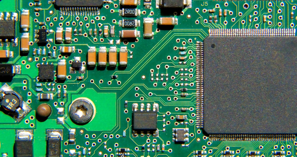
Printed Circuit Boards (PCB), are at the heart of modern electronics. They consist of layers of copper separated by an insulating material, often seen in green. They serve as a support to connect and hold components, with the goal of building an electronic board.
In this tutorial, you will learn how to use KiCad software to design a simple PCB, from the electronic schematic to the board layout ready for fabrication.
_For any comments or questions, feel free to email me at [ousmane.thiongane@outlook.com](mailto:ousmane.thiongane@outlook.com)._
## Requirements
* A computer with [KiCad](https://www.kicad.org/) installed
* That’s it!
## Goal
The goal of this tutorial is to create a small PCB with simple components (LEDs, buzzers, resistors, etc.) that can later be connected and used with a microcontroller board:
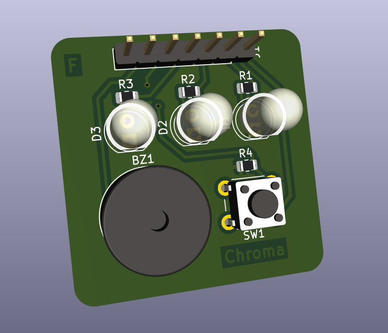
This project is carried out in two parts:
* **Schematic:** Here we draw the circuit schematic, just like in the [introduction to embedded programming.]({{< relref "tutorials/electronics/introduction_to_embedded_prog" >}}) You will find such schematics in electronics courses.
* **Routing:** This is where the position of the various components is chosen, and where they are connected together by routing.
## Schematic

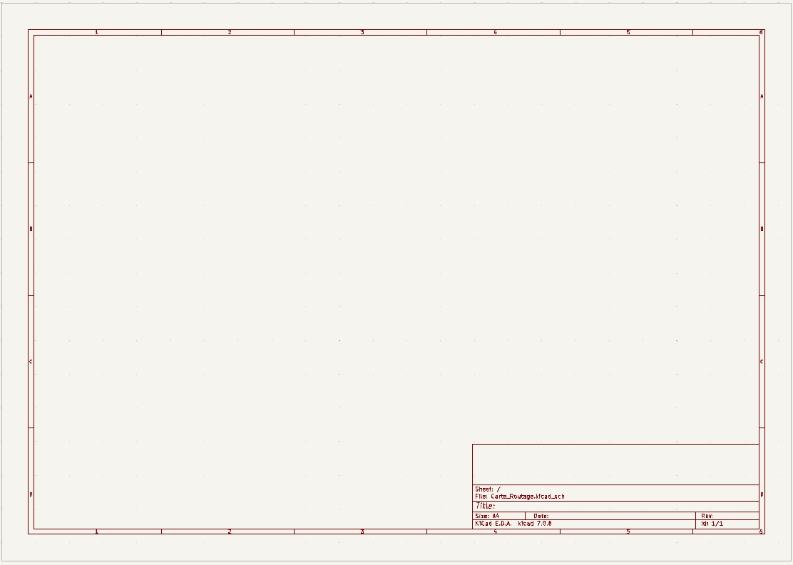
{{< callout context="note" title="Mission" icon="outline/target-arrow" >}}
**Create a new KiCad project, then open the "Schematic Editor" to get the page shown above.**
{{< /callout >}}
{{< callout context="caution" title="Tip" icon="outline/bulb" >}}
You can edit the title block at the bottom right of your schematic by double-clicking it. It’s common to add the date, version, title, your name, and comments, etc.
{{< /callout >}}
### Placing Components
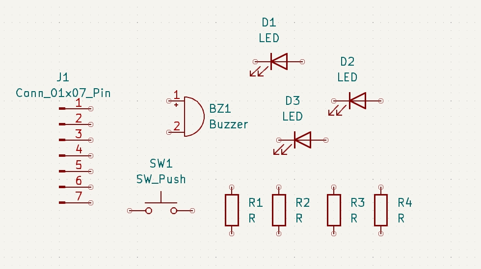
For our board, we need to place the following components on the page:
* 3 LEDs (LED)
* A 7-pin male connector (Conn_01x07_Pin)
* 4 resistors (R)
* 1 push-button switch (SW_Push)

{{< callout context="note" title="Mission" icon="outline/target-arrow" >}}
**Add all the required components to the schematic as shown above using the "Place Symbol" tool.**
{{< /callout >}}
{{< callout context="caution" title="Tip" icon="outline/bulb" >}}
The "A" shortcut key also opens the "Place Symbol" tool! For future missions, shortcuts will be provided in parentheses when available.
{{< /callout >}}
### Connecting Components
Now we will connect the components together with wires, and also using what are called labels.
Local and global labels allow you to connect components without drawing wires between them. This is very useful for improving readability in a large schematic. Here is an example without labels:
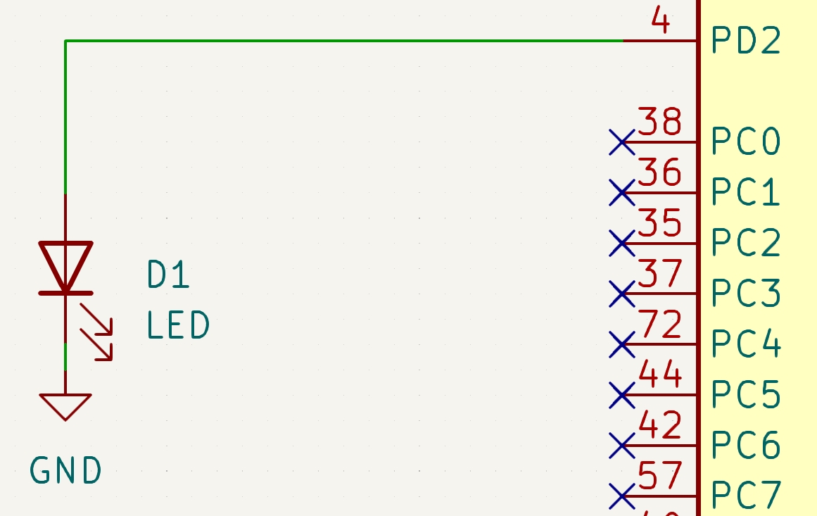
And the same schematic with labels (both are equivalent!):
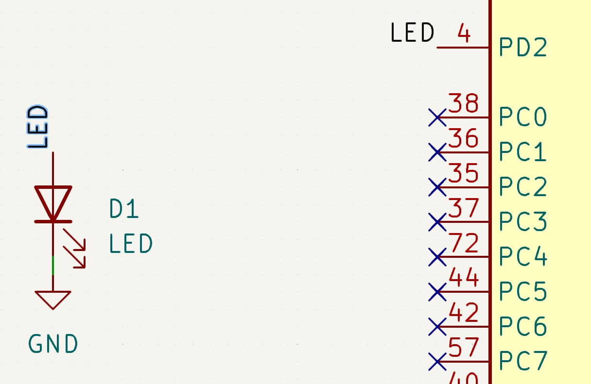
* **Local label:** Functional for a single page of the project (what we will use in this tutorial since we only have one page).

* **Global label:** Functional across all pages of the same project.

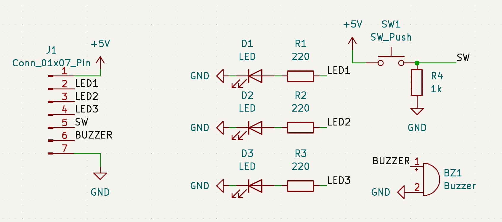
{{< callout context="note" title="Mission" icon="outline/target-arrow" >}}
**Connect the components with wires (W) and labels (L), and add the +5V power rail and GND ground (A).**
{{< /callout >}}
{{< callout context="tip" title="Did you know?" icon="outline/message-dots" >}}
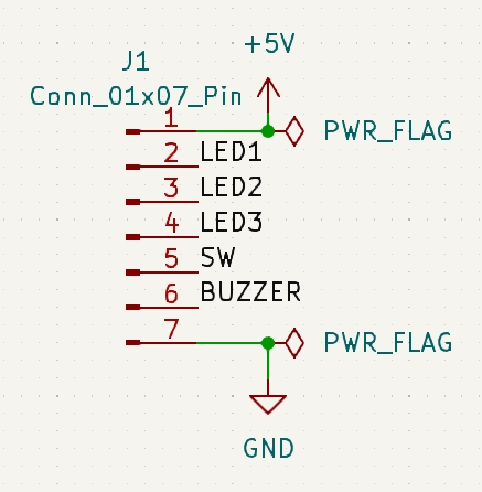
To avoid errors later during the Electrical Rules Check, place a power flag (PWR_FLAG) in parallel on +5V and ground, as shown below. This flag tells KiCad where the power is supplied from.
{{< /callout >}}
### Annotating Components
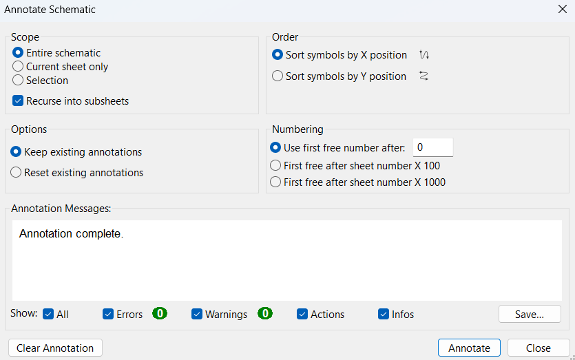
Next, we will assign unique reference designators to each component so they can be distinguished.

{{< callout context="note" title="Mission" icon="outline/target-arrow" >}}
**Use the "Annotate Schematic" tool to review and update the reference designators.**
{{< /callout >}}
### Electrical Rules Check
Your schematic is now complete, but you must verify that there are no errors. This is done with the Electrical Rules Checker (ERC).

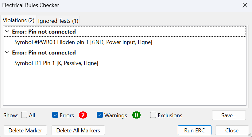
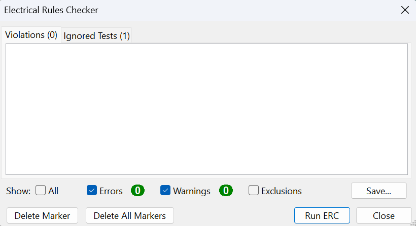
In the example above, a connection between LED D1 and ground was missing. We add the required wire, rerun the ERC, and the errors disappear:
{{< callout context="note" title="Mission" icon="outline/target-arrow" >}}
**Run the ERC and fix any errors until there are none left.**
{{< /callout >}}
### Assigning Footprints
Now we need to assign a footprint to each component, defining its shape and dimensions on the PCB. We do this with the "Assign Footprints" tool.

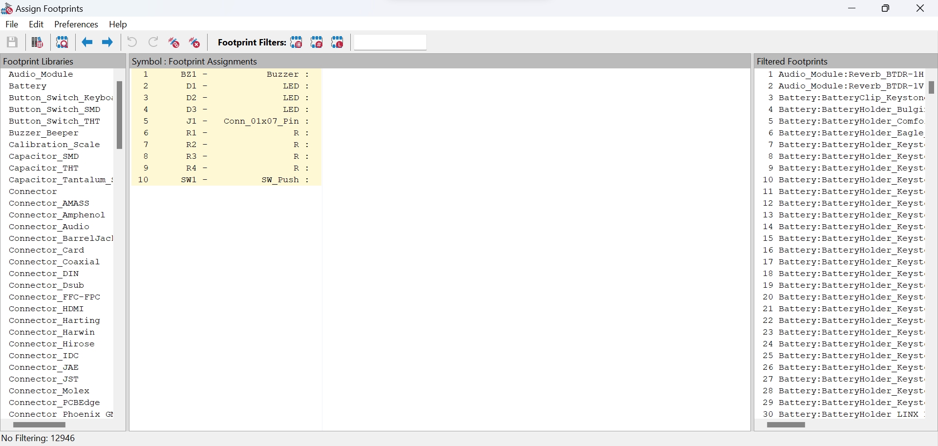
The tool is divided into three columns:
1. Available footprint libraries
2. Your schematic symbols and their currently assigned footprints (none yet)
3. The list of all footprints in KiCad
To avoid searching through all footprints, you can apply three filters:

1. Footprints defined for the selected symbol
2. Filter by pin count of the selected symbol
3. Filter by selected libraries in the left column
_In this example, you can enable all three filters at once by checking their boxes._
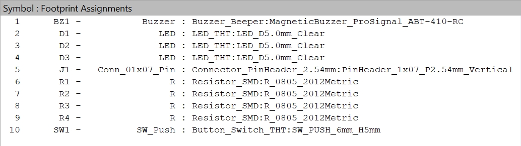
{{< callout context="note" title="Mission" icon="outline/target-arrow" >}}
**Assign the appropriate footprints to each component as indicated above.**
{{< /callout >}}
Once all footprints are assigned and the ERC shows no errors, we can move on to PCB layout in the next part.
---
## Credits
* **Writer:** [Ousmane THIONGANE](https://mowibox.github.io/)
* **Reviewer:** Loubna LATRECHE