# Introduction to printed circuit board design – Part 2Part 2 of the introduction to PCB design with KiCad: importing the schematic, routing traces, ground planes, net classes, and checking design rules.
## Requirements
* Completed [Introduction to printed circuit board design – Part 1]({{< relref "tutorials/electronics/introduction_to_pcb_design_part1" >}})
## Goal
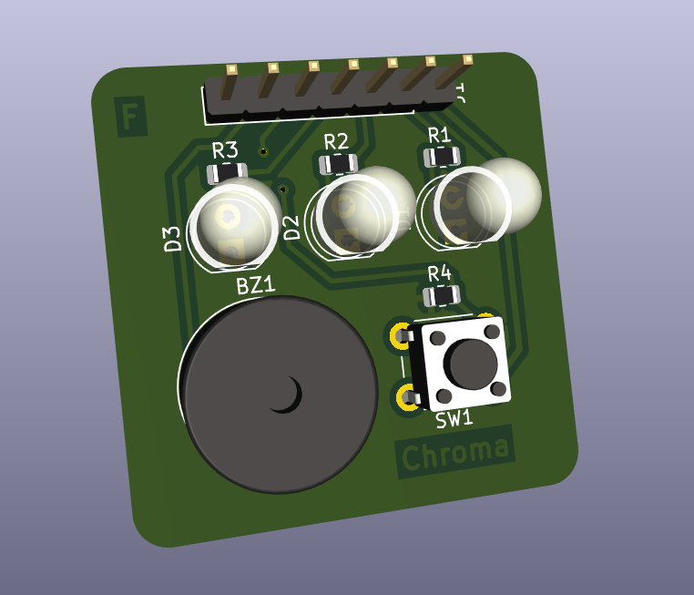
The goal of this tutorial is to build a small PCB with simple components (LEDs, buzzers, resistors, etc.) that can later be connected to and used with an electronic board.
In the previous section, we created the electrical circuit in the schematic editor. In this part, we’ll prepare the board for fabrication by arranging components and their connections on the PCB.
## Routing

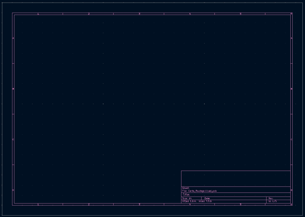
{{< callout context="note" title="Mission" icon="outline/target-arrow" >}}
**Open the KiCad "PCB Editor".**
{{< /callout >}}
### Importing Components

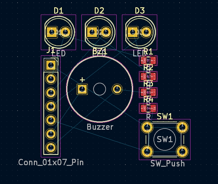
{{< callout context="note" title="Mission" icon="outline/target-arrow" >}}
**Import the components from your schematic into the PCB editor.**
{{< /callout >}}
### PCB Outline
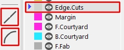
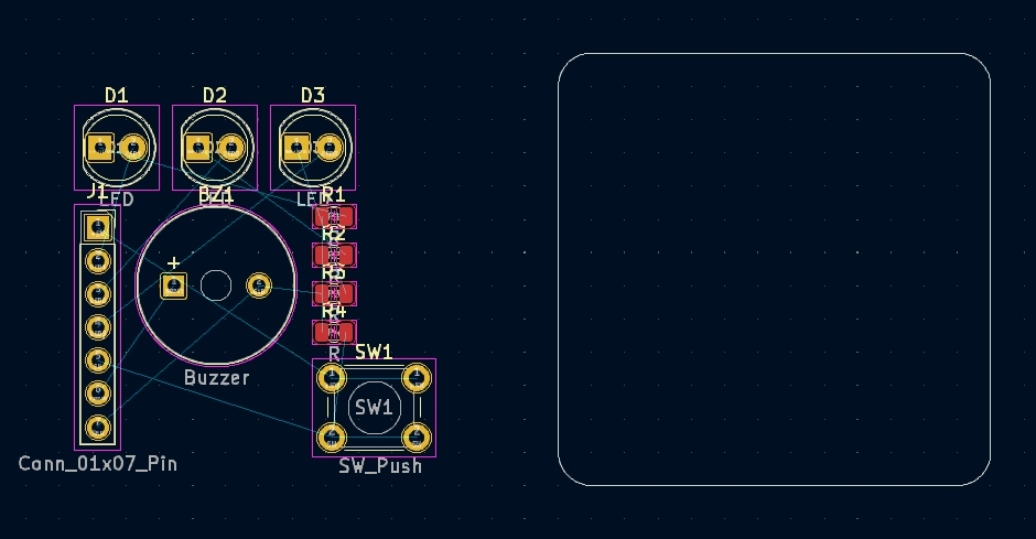
{{< callout context="note" title="Mission" icon="outline/target-arrow" >}}
**Select the "Edge.Cuts" layer and draw your PCB outline using the "Line" and "Arc" tools.**
{{< /callout >}}
{{< callout context="caution" title="Tip" icon="outline/bulb" >}}
Allow about a 30mm x 30mm square to fit all components inside. You can also make it smaller or fully round… No one says you must follow the example exactly!
{{< /callout >}}
### Ground Plane
The ground net is the most important signal on the PCB, as it spans nearly the entire board. We’ll create filled zones of this net, called ground planes. Adding ground planes on both sides of the PCB helps to:
* Minimize trace impedance
* Automatically connect grounded components
* Be more eco-friendly!

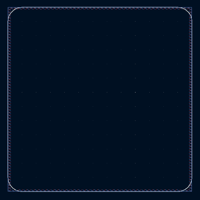
{{< callout context="note" title="Mission" icon="outline/target-arrow" >}}
**Select the "F.Cu" layer and click "Add filled zone". Choose "GND", confirm, and outline the PCB. Repeat on the "B.Cu" layer.**
{{< /callout >}}
### Component Placement
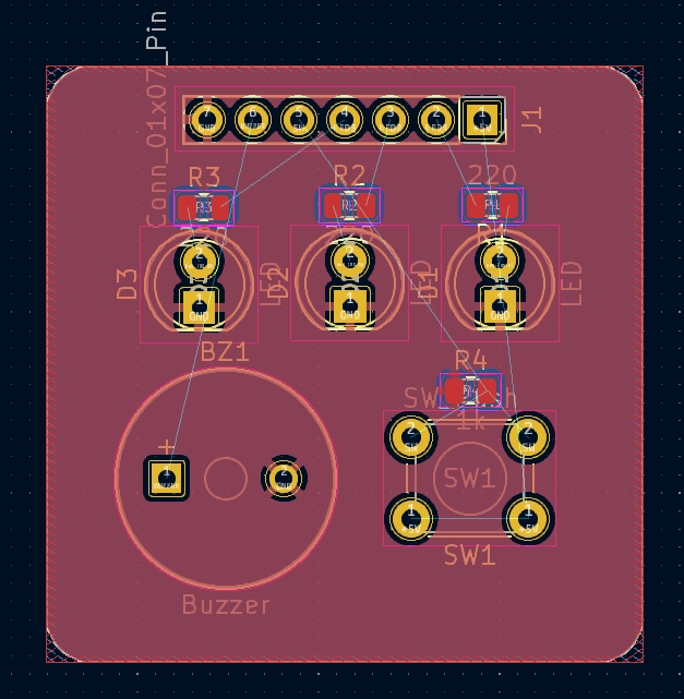
{{< callout context="note" title="Mission" icon="outline/target-arrow" >}}
**Place the components anywhere inside your board outline, then regenerate the ground plane (shortcut "B").**
{{< /callout >}}
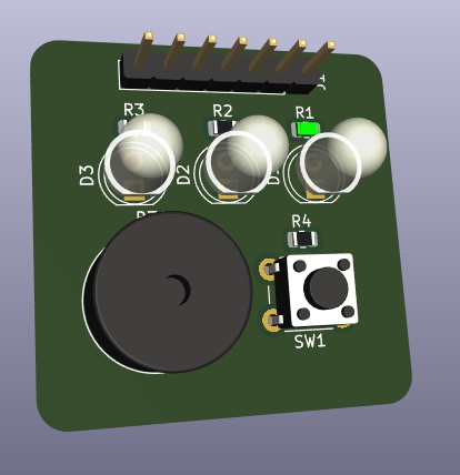
{{< callout context="caution" title="Tip" icon="outline/bulb" >}}
You can preview your board in 3D via the "View" menu → "3D Viewer". So pretty!
{{< /callout >}}
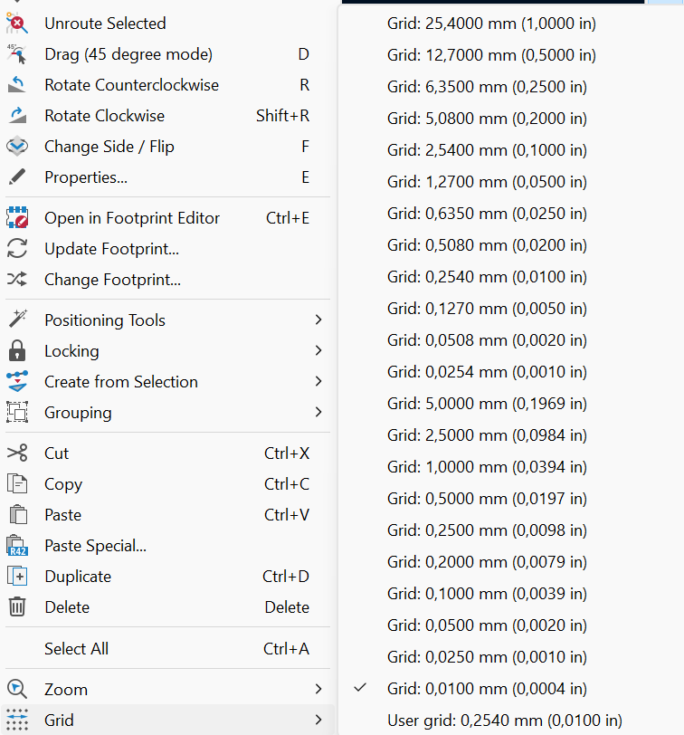
{{< callout context="tip" title="Did you know?" icon="outline/message-dots" >}}
Right-click on the workspace and select "Grid" to adjust the grid spacing for finer placement.
{{< /callout >}}
### Net Classes
Before routing, we must define net classes:
> _In electrical engineering, an equipotential set is a group of conductors at the same voltage, thus having no potential difference. An equipotential bonding aims to equalize voltage across a space._ [(Wikipedia - french)](https://fr.wikipedia.org/wiki/%C3%89quipotentielle#%C3%89lectricit%C3%A9)

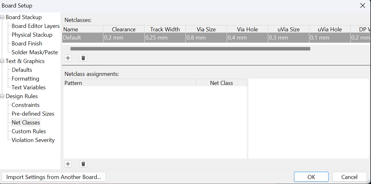
{{< callout context="note" title="Mission" icon="outline/target-arrow" >}}
**Go to "Board Setup" → "Net Classes" and update the "Default" class to:**
* **Clearance: 0.3 mm**
* **Track Width: 0.3 mm**
* **Via Size: 0.8 mm**
* **Via Hole: 0.4 mm**
{{< /callout >}}
Very often, the tracks carrying the circuit's power supply can carry higher currents. This leads to significant power dissipation. To fix this, we're going to create a net class dedicated to power supply signals (+5V or GND). These tracks will be wider to reduce track impedance.

{{< callout context="note" title="Mission" icon="outline/target-arrow" >}}
**Click the "+" button to create a "Power" class with:**
* **Clearance: 0.3 mm**
* **Track Width: 0.5 mm**
* **Via Size: 1.2 mm**
* **Via Hole: 0.6 mm**
{{< /callout >}}
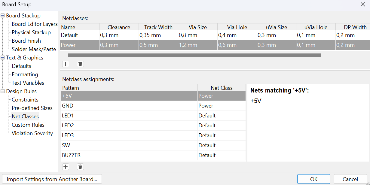
{{< callout context="note" title="Mission" icon="outline/target-arrow" >}}
**Using the second "+" button, add all nets (+5V, GND, LED1, etc.) and assign them to "Power" (for +5V and GND) or "Default" (others).**
{{< /callout >}}
### Where the “routing" introduction comes into its own

{{< callout context="note" title="Mission" icon="outline/target-arrow" >}}
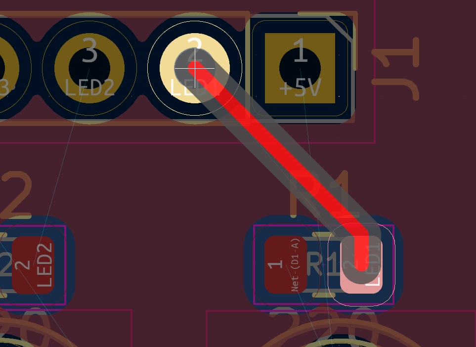
**Route all tracks as shown by the ratsnest (X).**
{{< /callout >}}
{{< callout context="danger" title="Warning" icon="outline/alert-square-rounded" >}}
Avoid 90° trace angles—they cause electromagnetic interference (EMI) and can degrade PCB performance.
{{< /callout >}}
{{< callout context="caution" title="Tip" icon="outline/bulb" >}}
If routing is difficult, try repositioning components or using the bottom layer "B.Cu". Feel free to experiment!
{{< /callout >}}
{{< callout context="caution" title="Tip" icon="outline/bulb" >}}
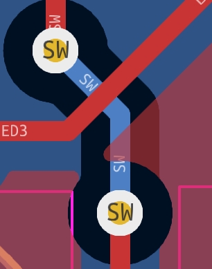
Another alternative would be to alternate between the two layers by passing through a “hole”. This is the role of a via. Press "V" while routing a track to drop a via and switch layers.
{{< /callout >}}

{{< callout context="caution" title="Tip" icon="outline/bulb" >}}
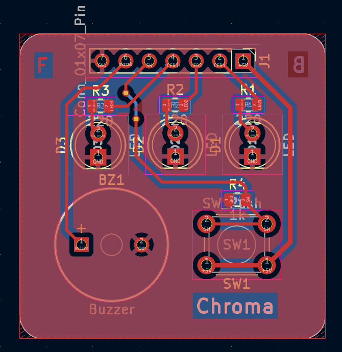
Add text to your board (Ctrl + Shift + T) and regenerate the ground plane for embossed lettering. Don’t forget to refill your zones when done!
{{< /callout >}}
### Design Rules Check
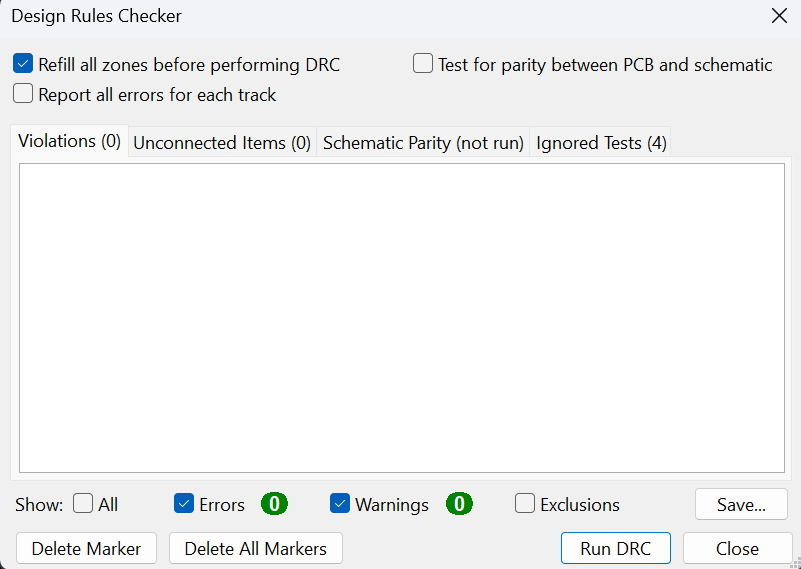
Just like the [ERC]({{< relref "tutorials/electronics/introduction_to_pcb_design_part1/#electrical-rules-check">}}) for schematics, we need to verify your routing with the Design Rules Checker (DRC).

{{< callout context="note" title="Mission" icon="outline/target-arrow" >}}
**Run the DRC and fix errors if any.**
{{< /callout >}}
**And there you have it—your finished PCB!**
## Going further
---
## Credits
* **Writer:** [Ousmane THIONGANE](https://mowibox.github.io/)
* **Reviewer:** Loubna LATRECHE